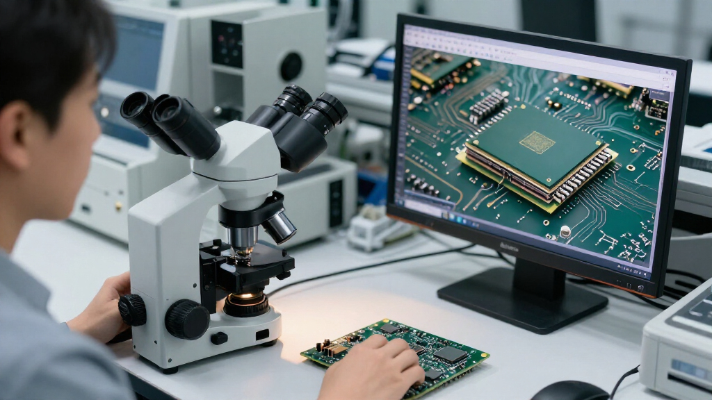
🔍 Read the full analysis: AI Chips Up Close: Understanding Dies, HBM And 3D Packaging on ThorstenMeyerAI.com

Get the latest gadgets delivered free with Prime
- Fast, free delivery on millions of items
- Prime Video, Amazon Music and more included
- Member-only deals all year
TL;DR
A November 22, 2026, explainer from ThorstenMeyerAI.com breaks down AI accelerators as packages combining compute dies, high-bandwidth memory and complex wiring layers—not single chips. The article says memory bandwidth and advanced packaging are important performance and production constraints, while the scale of future supply remains uncertain.
ThorstenMeyerAI.com published an AI-chip hardware explainer on November 22, describing how current accelerators combine multiple compute dies, stacked high-bandwidth memory (HBM) and silicon wiring layers inside one package. The report argues that memory bandwidth and advanced packaging, not just raw computing capacity, can shape accelerator performance and the number of systems manufacturers can deliver.
The article uses layer-by-layer 3D models to show a package from its base substrate to its cooling plate. Between those layers are a silicon interposer, which connects components with dense wiring; compute dies; and HBM stacks positioned close to the compute. HBM consists of DRAM layers connected vertically using through-silicon vias, or TSVs. The models are schematic in size: the article says manufacturers do not publish the dimensions needed to represent the components at true scale.
The report compares different accelerator designs. It says Nvidia’s Rubin GPU uses two reticle-limited compute dies and reports 336 billion transistors, citing Nvidia’s architecture blog. AMD’s MI350-series design combines eight stacked accelerator complex dies with two I/O dies; the article gives the MI355X a total of 185 billion transistors. It also says AMD’s next-generation MI455X and MI450X use stacked 3D hybrid-bonded compute dies, citing AMD.
The explainer places those packages in the context of complete systems. Nvidia’s GB200 and GB300 NVL72 racks are described as containing 72 GPUs and 36 CPUs, alongside compute trays, NVLink switch trays, networking and power equipment. It also cites Nvidia’s stated 120-kilowatt cooling capacity for a GB200 NVL72 rack. These configurations show that an AI system depends on more than the accelerator package: cooling, interconnects and rack-level integration are part of the design.
Memory and Packaging Set Limits
The report’s central point is that an accelerator’s compute dies need a steady supply of data. HBM bandwidth can limit how quickly a system feeds those dies, while the interposer and other packaging technologies provide the many connections needed between memory and compute. That makes packaging an engineering and manufacturing concern, not merely a way to hold chips together.
The article gives Nvidia product-page figures for memory bandwidth rising from 900 GB/s on V100 to 19.2 TB/s for Rubin. Those figures refer to different products and generations; they do not, on their own, establish how much faster a particular AI workload will run. Performance also depends on the workload, system configuration and software.
Packaging capacity also matters to supply. The source reports that SK hynix expects HBM demand to exceed supply through 2030. That is a company forecast, not a confirmed measurement of future shortages. If demand outpaces available memory and packaging capacity, chip availability and prices for AI infrastructure could be affected even when compute designs are ready.
Products Worth Considering

DJI Mic 3 Wireless Microphone (2 Transmitters, 1 Receiver, Charging Case)

Samsung 27-Inch Odyssey G5 QHD Gaming Monitor (G51F)

Samsung 32 Odyssey G5 QHD Gaming Monitor
As an affiliate, we earn on qualifying purchases.
From Interposers to Full Racks
A silicon interposer is a layer that provides dense connections among a package’s dies and memory stacks. The source describes TSMC’s CoWoS-S as using a large silicon interposer and cites the company’s stated capacity for interposers up to about 2,700 square millimeters, or 3.3 times the area of a standard lithography reticle. For larger packages, CoWoS-L uses silicon bridges within a carrier layer. The article cites TSMC’s statements that 3.5-reticle designs had reached volume production in 2024 and that it was producing 5-reticle designs in October 2026, while developing larger formats.
HBM stacks are also becoming taller. The source says JEDEC’s HBM4 standard, published in April 2025, allows stacks of four, eight, 12 or 16 layers and up to 64 GB per stack. Those are standard limits, not proof that every accelerator uses the maximum configuration. The article also cites SK hynix and Samsung descriptions of efforts to stack more memory layers while reducing chip thickness and spacing.
At rack scale, components must be cooled and linked as a system. The source says liquid cooling plates are attached to CPUs and GPUs in Nvidia’s rack design, while the GB200 NVL72 configuration combines compute trays with separate NVLink switch trays. The article’s stated configurations and measurements are drawn from vendor documents and an Open Compute Project listing, with model dimensions shown schematically.
“Where AI gets stuck today, it is often not the compute die. It is memory bandwidth, packaging, and how many of these parts the world can actually build.”
— ThorstenMeyerAI.com, November 22, 2026
Capacity Forecasts and Workloads
The source does not provide independently verified forecasts for how many accelerator packages the industry can produce, or how much packaging capacity will be available. Its statement that HBM demand may outpace supply through 2030 is attributed to SK hynix and should be read as a company outlook. The article also does not quantify the resulting effect on prices or delivery schedules.
Product specifications do not establish real-world performance across all AI workloads. The reported bandwidth figures and transistor counts come from vendor materials, and the article does not present comparative benchmark testing. It also says its 3D models use schematic dimensions because exact package and die sizes are not publicly provided. Actual configurations may differ by product, customer and system version.
Track Packaging and HBM Output
The next indicators will be whether manufacturers expand advanced packaging and HBM production, and whether announced accelerator designs enter broad availability in the configurations described. TSMC’s progress on larger interposers and suppliers’ HBM road maps will help show whether packaging and memory can keep pace with demand. The source provides no timetable or independently confirmed production totals for those expansions, so supply and delivery effects remain open.
Key Questions
What is an AI accelerator package?
It is the assembled unit that can include compute dies, HBM stacks, an interposer and a package substrate. The components work together; an accelerator is not necessarily one piece of silicon.
What does HBM do?
High-bandwidth memory stores data close to the compute dies. Its stacked DRAM layers use vertical connections called TSVs, helping provide high data bandwidth within the package.
Why does an AI chip need an interposer?
A silicon interposer provides dense wiring between compute dies and memory stacks. The source describes advanced interposer packaging as a production constraint as well as a design feature.
Does higher memory bandwidth guarantee faster AI?
No. Bandwidth is one factor in performance. Results also depend on the model, workload, software and full system configuration; the cited product specifications are not comparative workload benchmarks.
Is an HBM shortage through 2030 confirmed?
No. The source attributes that outlook to SK hynix. It is a company forecast that demand will exceed supply, not confirmation of future shortages or their size.
Source: ThorstenMeyerAI.com